Arizona Branch Office
TEL: (917)794-8330
EMAIL: sales@leadinway.com.tw
Address: 1 W Deer Valley Rd., suite 203, Phoenix, Arizona 85027
Arizona Branch Office
TEL: (917)794-8330
EMAIL: sales@leadinway.com.tw
Address: 1 W Deer Valley Rd., suite 203, Phoenix, Arizona 85027
AI is changing not only how chips are designed, but also how they are packaged, connected, cooled, and manufactured.
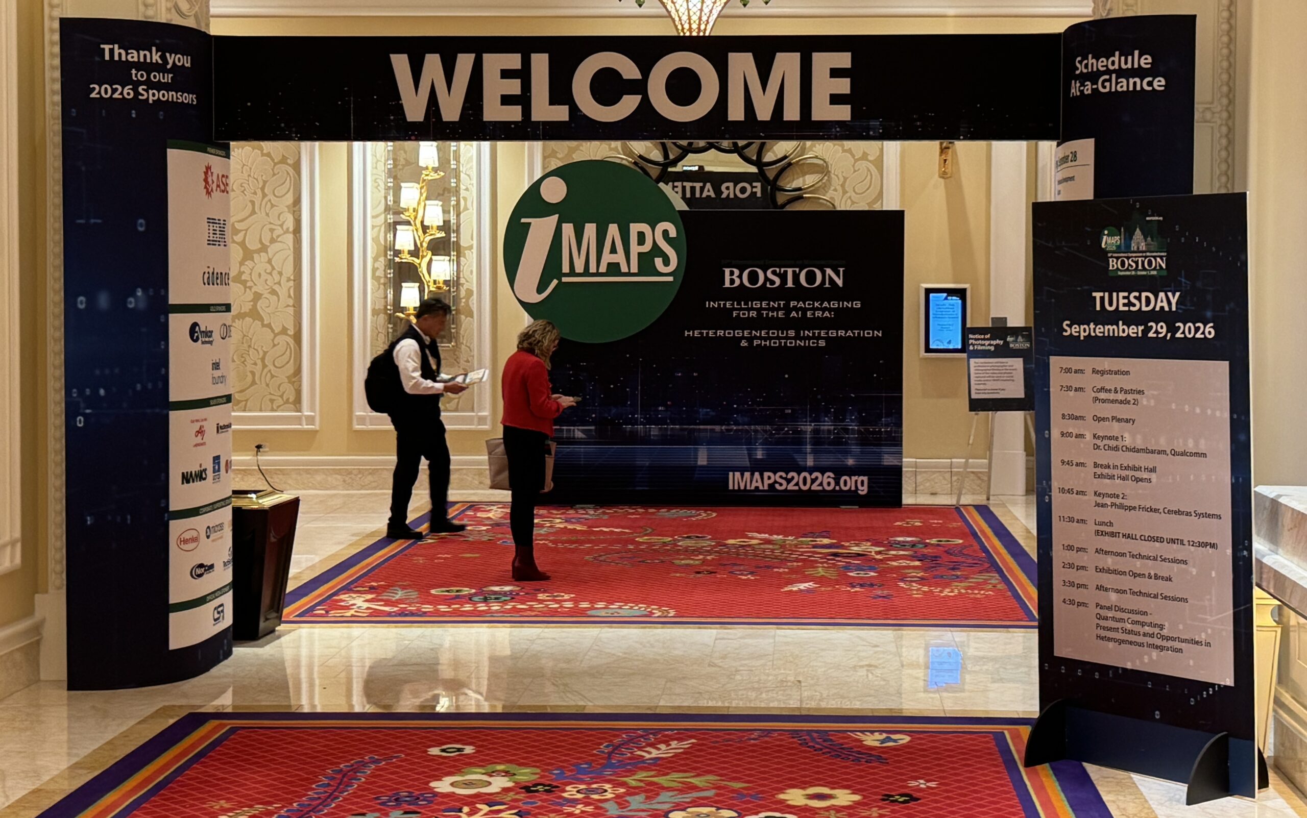
At IMAPS 2026, the 59th International Symposium on Microelectronics, advanced packaging took center stage under the theme “Intelligent Packaging for the AI Era: Heterogeneous Integration and Photonics.”
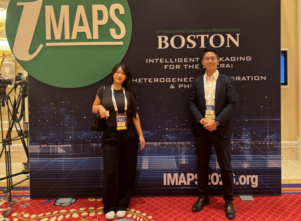
Here are four advanced packaging trends worth watching:
1. Heterogeneous Integration Takes Center Stage
As semiconductor manufacturing becomes increasingly complex, heterogeneous integration provides another path to higher system performance.
Instead of placing every function on one large monolithic die, designers can combine specialized chiplets within a single advanced package.
This shift creates new requirements across bonding, inspection, materials, testing, and precision assembly, making packaging increasingly critical to device performance and reliability.
2. Hybrid Bonding Pushes Interconnect Density Higher
As chiplets move closer together, hybrid bonding is higher interconnect densities for next-generation 2.5D and 3D packaging.
High-volume manufacturing, however, requires extremely precise alignment, surface preparation, contamination control, metrology, and process control.As dimensions continue to shrink, inspection becomes even more critical.
LeadinWay USA provides advanced AOI solutions helping manufacturers detect process deviations and defects during advanced packaging assembly.
3. Co-Packaged Optics Addresses the Data Bottleneck
AI systems do more than compute enormous amounts of data—they must also move it.
Increasing bandwidth requirements are accelerating the development of silicon photonics, optical I/O, photonic chiplets, and co-packaged optics (CPO) to address of conventional electrical interconnects.
At the same time, AI infrastructure is driving innovation in compound semiconductors, including GaN for high-performance power and high-frequency applications.
LeadinWay supports this evolving ecosystem with GaN testing/characterization solutions for next-generation compound semiconductor development and manufacturing.
4. Thermal Management Becomes a Design Priority
More compute density also means more heat.
For advanced 2.5D and 3D packages, thermal management can no longer be an afterthought.
IMAPS 2026 highlighted advanced thermal interface materials (TIMs) and material approaches including graphite, graphene, diamond-based materials, and sintered metal pastes to improve heat transfer and package reliability.
What Comes Next for Advanced Packaging?
The takeaway from IMAPS 2026 is clear: semiconductor performance increasingly depends on more than transistor scaling.
Chiplets, heterogeneous integration, hybrid bonding, photonics, advanced materials, and thermal management are evolving together, creating new opportunities across the advanced packaging ecosystem.
Connect with us
LeadinWay USA have continued to invest in and build experience across the advanced packaging ecosystem, working with technology partners and semiconductor manufacturers across the U.S. and Asia.
Looking for semiconductor manufacturing solutions or opportunities for you advance packaging roadmap? Contact LeadinWay USA to start the conversation.