Arizona Branch Office
TEL: (917)794-8330
EMAIL: sales@leadinway.com.tw
Address: 1 W Deer Valley Rd., suite 203, Phoenix, Arizona 85027
Arizona Branch Office
TEL: (917)794-8330
EMAIL: sales@leadinway.com.tw
Address: 1 W Deer Valley Rd., suite 203, Phoenix, Arizona 85027

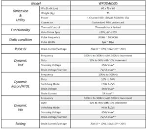
| Model | WPDDA6505 | |
|---|---|---|
| Dimension & Utility | W x D x H (cm) | 60 x 70 x 60 |
| Weight (Kg) | 75 | |
| Power | 1 Channel 100-120VAC 50/60Hz 15A | |
| Connector | Customized Mini probe card | |
| Functionality | Thermal Control | Thermal chuck limited |
| Gate Driver Spec | ±20V, ΔV ≤ 20V | |
| Static condition | Pulse Frequency | 200Hz ~ 10000Hz |
| Pulse Width | 1µs ~ 10µs | |
| Pulse IV | Drain Current/Voltage | 20A (0 ~ 10V), 10A (10V ~ 20V) |
| Dynamic Vsd | Frequency | 100kHz to 300kHz with 100kHz Increment |
| Duty | 10% to 90% with 10% increment | |
| Stressing Voltage | 650V max* | |
| Drain Voltage/Current | 7V/5A max** | |
| Dynamic Rdson/HTOL | Frequency | 10kHz to 300kHz |
| Duty | 10% to 90% | |
| Switching Mode | HSW & ZVS | |
| Drain Voltage | 650V max* | |
| Drain Current | 5A max** | |
| Dynamic Vth | Frequency | 100kHz to 300kHz with 100kHz Increment |
| Duty | 10% to 90% with 10% increment | |
| Switching Mode | HSW & ZVS | |
| Stressing Voltage | 650V max* | |
| Drain Voltage/Current | 2V/5A max** | |
| Baking | Drain Current/Voltage | 20A (0 ~ 10V), 10A (10V ~ 20V) |
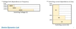
* Voltage limit dependence on Frequency: 650V (up to 100kHz), 500V (up to 200kHz), 400V (up to 300kHz).
** Switching current dependence on Duty: 5A (up to 20% duty), 4A (up to 40% duty), 3A (up to 90% duty).